Guided reading
Recently, Professor Tan Hairen's team from College of Engineering and Applied Science of Nanjing University cooperated with the research group of Trina Solar's State Key Laboratory of Photovoltaic Science and Technology have realized the high-quality conformal growth of wide-band gap perovskite films on industrial textured silicon substrates through technical innovation in the direction of structural design of top-bottom cells and process optimization. And they obtained a stabilized PCE of 28.6% (certified 27.9% from Fraunhofer-ISE) for perovskite/silicon heterojunction tandems. This work has been published in Advanced Materials in the title of "Efficient Perovskite/Silicon Tandem Solar Cells on Industrially Compatible Textured Silicon".
Research background
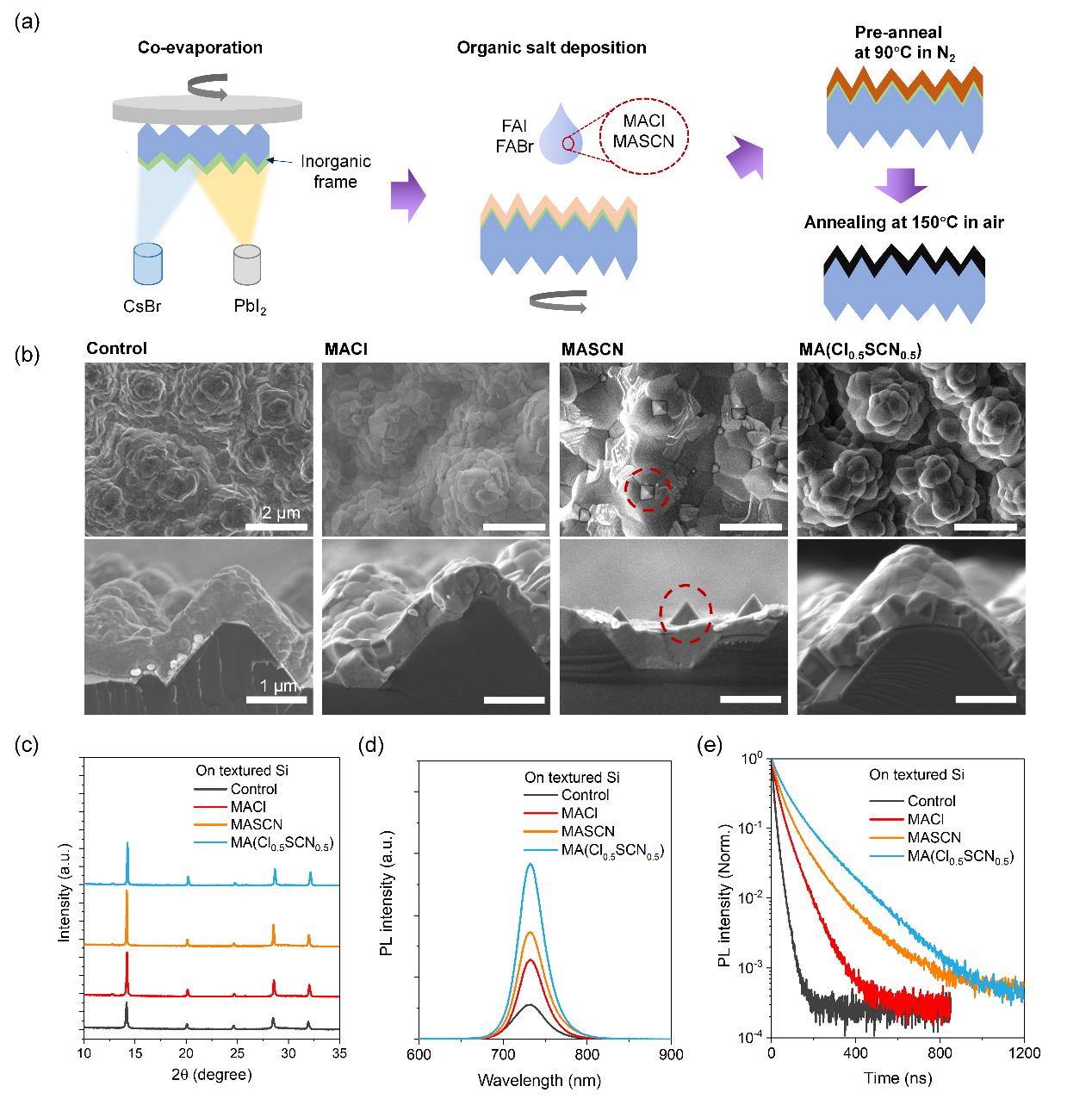
Monolithic perovskite/silicon tandem solar cells promise power-conversion efficiencies (PCEs) exceeding the Shockley-Queisser limit of single-junction solar cells. By combining evaporation and solution method, namely the hybrid two-step method (as shown in Figure 1a), conformal growth of perovskite film can be realized on the surface of industrial silicon cells, so as to make use of the great optical trapping characteristics of the pyramid structure of silicon, and achieve a high short-circuit current density. However, the growth quality of perovskite films prepared by the hybrid two-step method is generally poor compared with the all-solution method.
Research content
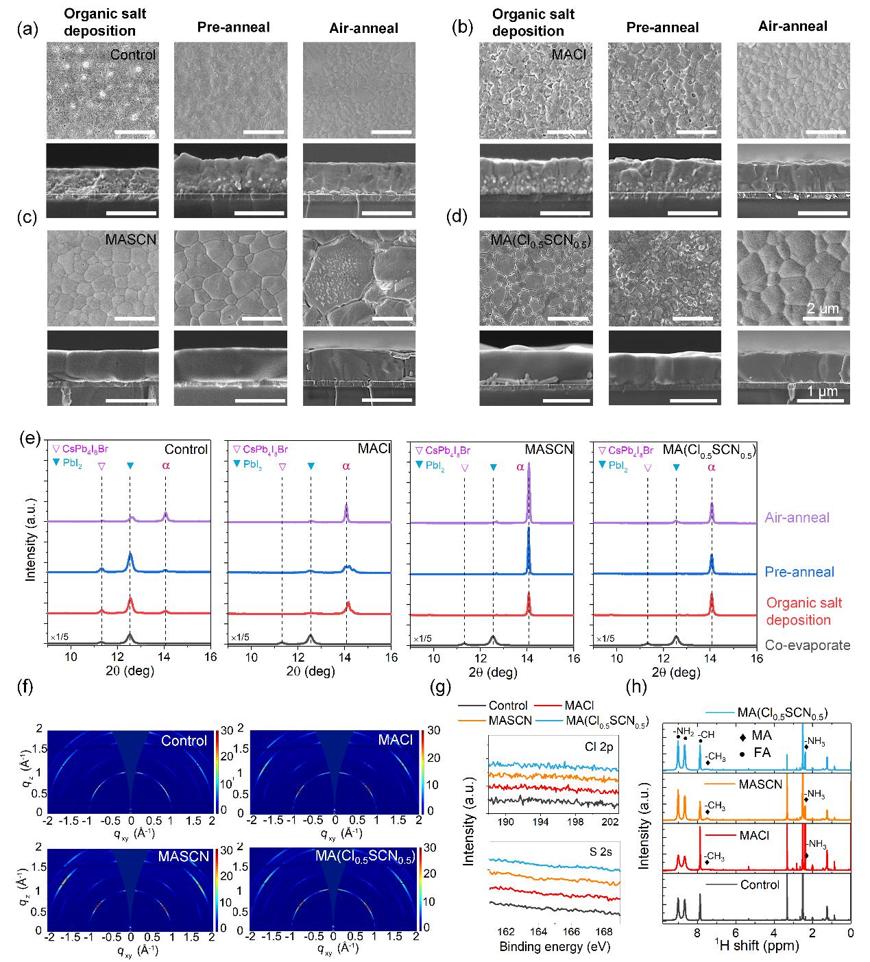
To solve the above problem, Tan's team and collaborators developed an organic anion additive assisted crystallization strategy, which introduced two organic salts, MACl (methylamine chloride) and MASCN (methylamine thiocyanate), into the solution spin-coating step of the hybrid two-step process. The reaction between the inorganic framework of PbI2 (lead iodide) prepared by evaporation and the organic components in the precursor solution was effectively regulated. And the conformal deposition of perovskite films with larger grains, lower trap density, and suppressed light-induced phase segregation was realized on the industrial texture silicon. By comparison, it is found (figure 1b, c, d) that without any additives, the reaction of perovskite is insufficient and the crystallinity is poor. MACl can merely promote the reaction and crystallization. MASCN can significantly improve the growth rate and size of grains by inducing crystal reconfiguration, but too large grains cannot achieve good conformal growth along the crystalline silicon surface. The combination of the two additives can give full play to their advantages and achieve the deposition of high quality perovskite thin films.

Figure 1. The conformal deposition of perovskites on industrially textured silicon. a) Schematic of the hybrid two-step deposition method. Anion-engineered additives including MACl, MASCN, or a mixture of MACl and MASCN are introduced to regulate the perovskite crystallization process. b) Top-view (up) and cross-sectional (down) SEM images of perovskite thin films without (control) and with different additives (MACl, MASCN, and MA(Cl0.5SCN0.5)) on textured silicon (average pyramid size >3 µm). XRD patterns (c), steady-state PL spectra (d), and time-resolved PL transients (e) of perovskite films on textured Si.

Figure 2. Characterization of perovskite films with different additives. a, b, c, d) Top-view (up), and cross-sectional (down) SEM images showing the conditions of perovskite films after different processes. e) X-ray diffraction (XRD) patterns of perovskite films after different process, including inorganic framework after co-evaporation (black line), organic salt deposition (red line), pre-annealing (blue line), and air-annealing (purple line). The symbol α represents α-phase perovskite. f) GIWAXS patterns of perovskite films with various additives. g) Cl 2p and S 2s XPS spectra of perovskite films. h) 1H NMR spectra of powders scratched from the perovskite films with various additives.

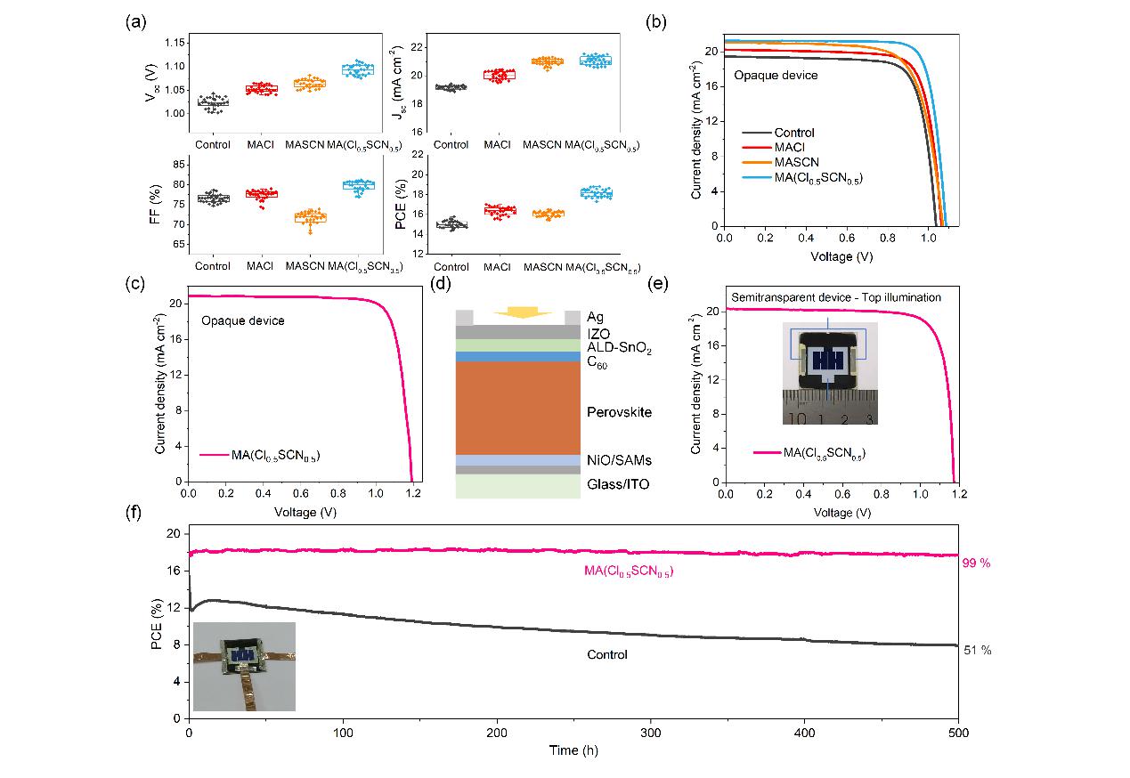
Figure 3. Photovoltaic performance of PSCs with varied additives. a) Photovoltaic parameters (Voc, Jsc, FF, and PCE) derived from 30 opaque devices. b) J–V curves of the champion opaque devices (0.049 cm2 aperture area). c) J–V curve of the champion opaque device with MA(Cl0.5SCN0.5) and surface passivation. d) Schematic view of the semitransparent cells illuminated from IZO side. e) J–V curve of the champion semitransparent cells with MA(Cl0.5SCN0.5) (aperture area of 1.05 cm2). f) Maximum power point (MPP) tracking of an encapsulated semitransparent cell.

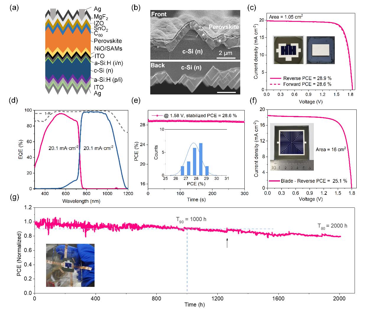
Figure 4. The device characterization of fully textured perovskite/Si tandems. a) Schematic diagram of perovskite/ SHJ tandem solar cell. b) Cross-sectional SEM images of perovskite/SHJ (average pyramid size >3 µm) tandem with MA(Cl0.5SCN0.5) additive. c) J–V curves of the tandem device (1.05 cm2 aperture area). d) EQE spectra of a current-matched fully textured monolithic perovskite/SHJ tandem cell. e) MPP tracking of the tandems and PCE distributions. f) J–V curves of the large-area tandem device (16 cm2 aperture area). g) MPP tracking of encapsulated tandem solar cells.
Consequently, they fabricated efficient perovskite/ silicon tandem solar cells employing the industrially feasible double-side textured silicon with pyramids over 3 µm, reaching an impressive efficiency of 28.9% (active area of 1.05 cm2) with a certified value of 27.9%. The corresponding Jsc value was up to 19.8 mA cm−2. The encapsulated tandem exhibited superior operation stability, maintaining over 80% of its initial output after over 2000 h MPP tracking. They also demonstrated that this strategy is compatible with the up-scaling process by employing the blade coating method, the tandems with a large aperture area of 16 cm2 achieved an efficiency of 25.1%, which is one of the highest reported values for perovskite/silicon tandem with an area over 10 cm2. The efficient strategy proposed herein could be widely applied in the commercialization of PSCs.
X.L., H.L., Dr. H.L. and Dr. R.X. contributed equally to this work. This work was financially supported by the National Natural Science Foundation of China (U21A2076, 61974063), Natural Science Foundation of Jiangsu Province (BK20202008, BK20190315), Fundamental Research Funds for the Central Universities (0213/14380219; 0213/14380218; 0213/14380216; 0205/14380252), the Research Funds for the Frontiers Science Center for Critical Earth Material Cycling, Nanjing University, and Program for Innovative Talents and Entrepreneur in Jiangsu. The research has also received funding from China Postdoctoral Science Foundation (2022M712341), Jiangsu Planned Projects for Postdoctoral Research Funds (2021K084A), and Science and Technology Support Plan (Industrial) Project of Changzhou City (CE20220032).
相关链接:https://doi.org/10.1002/adma.202207883

