Recently, A.P. Mingwei Zhu of College of Engineering and Applied Science, working with Prof. Liangbing Hu of University of Maryland, realized nanostructures on wood surfaces for the first time and demonstrated the ability to fabricate fine patterns on a wood surface, which greatly expands the conventional applications of wood. The manuscript titled as Precision Imprinted Nanostructural Wood is published on the famous material journal Advanced Materials. In the meanwhile, Nature highly praised the progress with Don’t knock wood: an ordinary material goes high-tech.

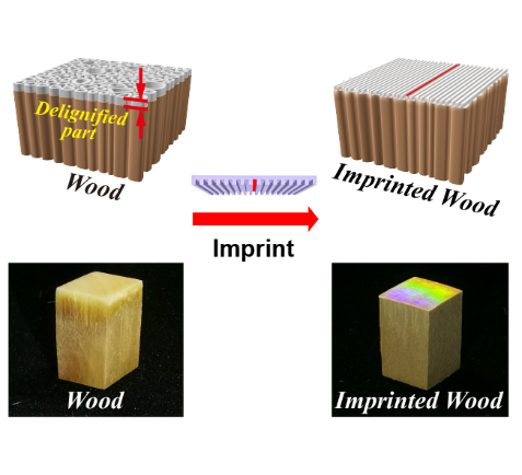
Figure 1 Schematic of the fabrication of the nanostructures on wood surface
Improving the functionality and performance of natural materials and promote their modern applications will give considerable impetus to the sustainable development of society. Wood is endowed with great biodegradability and has abundant sources. Nevertheless, plants is restricted by their sizes, defects, essential needs for life and many other things for a long time. As a result, their performance fail to meet modern requirements, which limits their applications only to traditional areas such as architecture and furniture for a long time. Surface micro- and nano-structures are the foundation of many optical and photonic devices. Realizing fabrication of nanostructures on wood surfaces will enable its applications in optical or photonic materials and devices as well as completely biodegradable, disposable environmental friendly materials and devices. However, wood is a highly porous structure formed mostly by aligned longitudinal cells. With such rough surface at micron scale, nanostructures are hard to form. To make it worse, cellulose which is the main gradient of wood shows no thermal plastic deformation property. Therefore, it remains a challenge to realize precise nanostructures on wood surface.
Addressing above research goal and challenge, the research group started from the hierarchical structure of wood/fiber and plastic-like behaviour of wood was observed. Then, imprinting on wood surface in wet condition at room temperature was implemented. After drying, hydrogen bonds between fiber were reformed. Afterwards, desired nanostructures were completely and precisely constructed on the wood surface. By then, construction of precision patterns from tens of nanometers to tens of micrometers on the surface of wood was realized.
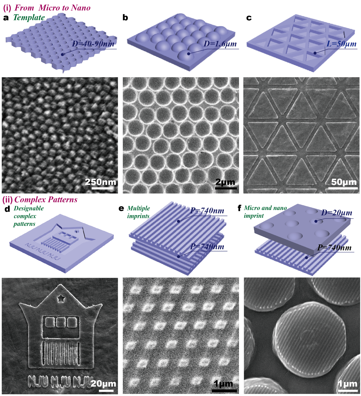
The research group successfully fabricated imprinting patterns with size ranging from 40 nm(hemispheres) to 50 μm. From the high resolution and fidelity of the patterns, it could be seen that this technique is able to obtain complicated and multiscale nanostructures with high efficiency. Through multiple imprinting, the research group fabricated 2D nanodot arrays using single-line-based mold. In other words, complicated pattern and mutiscale complex structures can be fabricated on wood surfaces with finite imprinting and limited mold types.

Figure 2 Demonstration of the patterning abilities on the surface of delignified wood using various templates. The surface patterns on wood can cover a wide range of scales, from nano to tens of micrometers.a) surface patterns of nanosized dots of ≈40-90 nm in size; b) Surface patterns of microcaves of ≈1.6 µm in diameter; c) Triangular embossments of ≈50 µm in side length.;
d) The patterns of the NJU logo on the wood surface. e) 2D dots array can be fabricated using a single line template by imprinting the wood twice at a different angle. f) Multiscale structures of microsized hemispheres with nanolines on their surfaces can also be achieved through double imprinting.

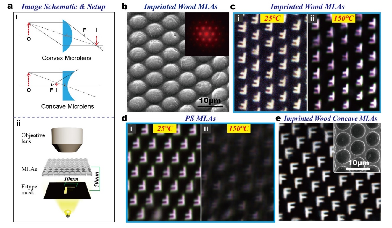
Figure 3 Application demonstration of the imprinted wood as an MLA. a) Schematic of the optical imaging setup using the MLA and its characterization with a microscope, in which the image effect is demonstrated using the character “F” as the objective. b) SEM image of the convex wood MLA with unit lens size of ≈6.5 µm in diameter. The inset is the light scattered dot pattern. Their periodic arrangement indicates the periodicity of the MLA over a large area. c) The image effect of the wood MLA, in which the clear images of the letter “F” with sharp edges are clearly observed. d) In contrast, the PS MLA does not show a clear image at 150 °C. e) The concave wood MLA also exhibits good image effect.
The research group also fabricated a wood microlens array (MLA) to demonstrate its potential in optical materials and technologies. Both the convex and concave MLA were fabricated and their imaging performance was characterized by using a projection via optical microscope. As is shown in Fig. 3, miniaturized images of letter “F” are clearly identified, demonstrating the good imaging ability of the wood MLA. Compared with conventional MLA material PS, wood MLA shows better thermal stability. At a temperature of 150 °C, the wood MLA can work without any image deformation. Fabrication of nanostructures on wood surface may open new possibilities for wood applications, such as biodegradable and green optics, biology, and electronics.
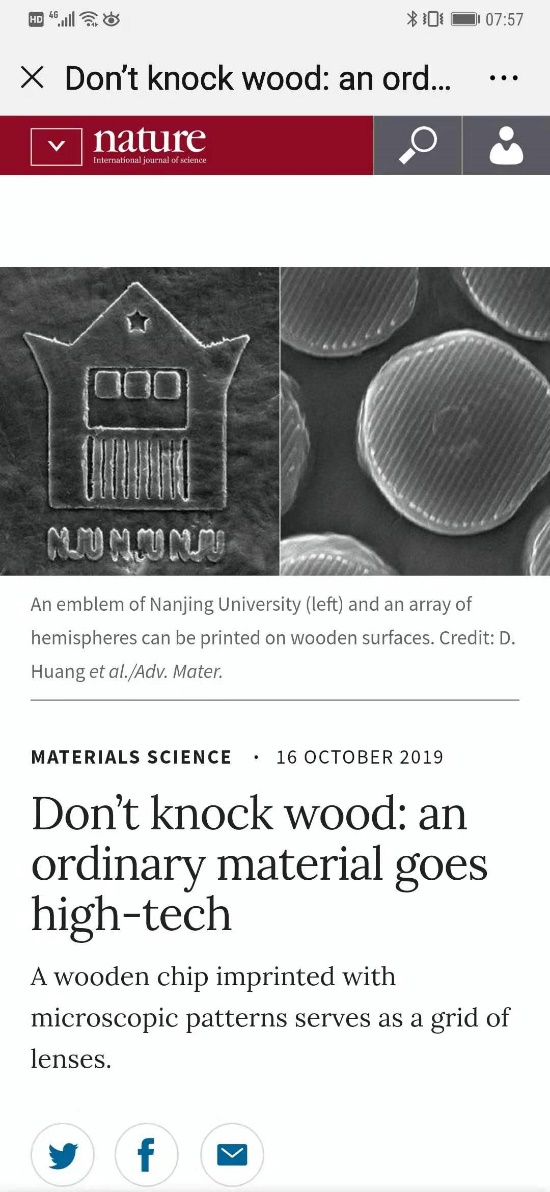
Nature Highlights the progress inDon’t knock wood: an ordinary material goes high-tech(https://www.nature.com/articles/d41586-019-03138-7):Mingwei Zhu at Nanjing University in China, Liangbing Hu at the University of Maryland in College Park and their colleagues have applied the technique to cellulose in wood fibre, which can serve as an abundant substitute for plastic.

Grade 18 doctor student Dafang Huang of Prof. Yanfeng Chen in our department, postgraduate Jiayang Wu, and postdocor Chaoji Chen of University of Maryland are the joint first authors of the paper. The co-corresponding authors are A.P. Mingwei Zhu of College of Engineering and Applied Science and Prof. Liangbing Hu of University of Maryland. The paper received close support from Prof. Haixiong Ge and A.P. Changsheng Yuan of our department.

