Prof. Min Han’s research group made important progress in high resolution and high sensitivity pressure sensor. The manuscript tilted as An ultrahigh resolution pressure sensor based on percolative metal nanoparticle arrays is published on Nature Communication (Nature Communication 2019, 19, 4024) on 6th September 2019. The corresponding author’s affiliation is Nanjing University and the first author is PhD student Minrui Chen. The corresponding author is Prof. Min Han of Nanjing University. This work also received the guidance and support from Academician Guanghou Wang.
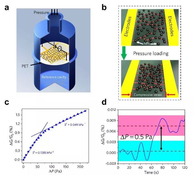
A precise pressure sensor is one of the most fundamental sensor devices in the microelectro-mechanical systems (MEMS), and has various applications in aerospace, autonomous driving, environment detection, and commercial electronic products. At present, the majorityof commercial pressure sensors used are silicon-based sensors. Itutilizes the piezoresistive or piezoresistive properties of doped silicon to sense changes of outside air pressure. However, due to the very high modulus of elasticity of silicon-based materials, the resolution of manufactured pressure sensors around atmospheric pressure is only ~ 100 Pa. Such a resolution is difficult to satisfy the needs of applications such as precise meteorological measurement and precise three-dimensional positioning. Therefore, on the one hand, the research groupreplacedsilicon wafers with polymer organic films with lower elastic modulus. On the other hand, they realized controllable preparation of nanoparticles (NP)arrays with quantum percolation and Coulomb blockade effects on flexible membrane by a nanocluster deposition technique, and converted the surface strain caused by pressure into the change in quantum tunneling conductance of NP arrays.
Compared with conventional silicon-based materials, the sensor has the following characteristics:
(1) Under a same pressure, a flexible polymer film with a lower elastic modulus is used as the pressure sensing device, and the surface strain will be much higher than that of the silicon wafer;
(2) In the dense NParrays attached to the film, the electronic transport is mainly realized by single-electron tunneling hopping, so that the dependence of tunneling conductance G of the NP arrayswith the average NP plane spacing d shows an exponential relationship, where β is the electronic coupling term, which is related to size and temperature. Therefore, even the slight surface strain of flexible membraneinduced by tiny pressure, which results in a very small change in the spacing of the NPs, is able to quickly shift the conduction state of the single-electron tunneling junction between the NPs. Along with thelarge number ofpercolation paths in the NP arrays,the sensitivity to the altitude influenced by the increase or decrease in the electrical conductivity of the NP arrays is very high.
(3) Moreover, the Coulomb Blockade effect in the NParrays can further reduce the current thermal noise caused by thermal fluctuations, thereby further further reducing the measurable minimum conductance change of the NP array. These factors have greatly improve the resolution and sensitivity of the pressure sensor.

Figure 1 (a) Schematic of the structure of the fabricatiedNP array pressure sensor based on a nanocluster deposition technique;(b) The operating principle of the sensor: When a pressure is loaded, the number of the percolation pathways (represented by red lines) are changed;(c) Dependence of the conductance of NP arrays with pressure;(d) Dependence of the conductance of NP arrays in response to a pressure change of 0.5 Pa.
The research group used a mask coating method to print interdigital electrodes (IDEs) on a 0.05mm thick polyethylene terephthalate (PET) material. Using the nanocluster deposition system, the controllable preparation of metal NP arrays between the IDEs was achieved. Finally, the PET membranewasencapsulated on a reference cavity to complete the preparation of the pressure sensor. When the pressure sensor is placed under different ambient pressure, the external pressure and the internal pressure of the reference cavity form a new mechanical balance on the PET membrane. The strain of the PET membrane will change the tunneling conductance of the NP arrays and be measured by a electrical circuit. The sensitivity of the pressure sensor reaches 0.13 kPa-1, and the pressure change as small as 0.5 Pa can be detected in an atmospheric pressure environment (Fig. 1) (compared with the current general silicon-based sensor, the resolution is improved by more than 3 orders of magnitude, and it is far beyond the pressure sensors made of other materials).
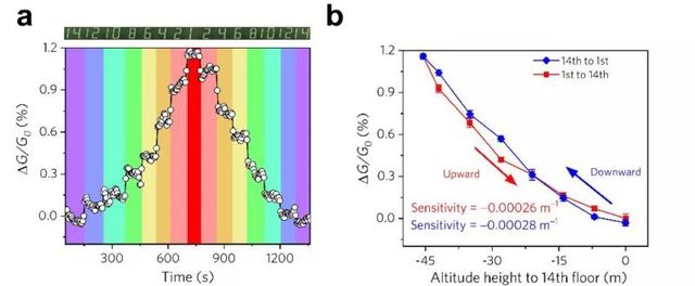
Forempirical verification, the research group further applied the pressure sensors to the measurement of air pressure changes at different altitudes. In a 14-story building elevator, the response of the sensors to different floors was recorded in real time. Experiments show that the sensor can distinguish the pressure change caused by 1 m altitude difference. As a barometric altimeter, the sensor can achieve a sensitivity of 0.00027 m-1 (Fig. 2). Such a ultra-high resolution barometric altimeter has important applications in aerospace and 3D global positioning systems.

Figure 2 (a) Realtime conductance changes in response to the variation in the floor elevation;(b) Summary of the data in (a) ,the elevation of each floor is converted into a height difference with respect to the 14th floor (calculated by the height of 3.5 meters per floor)
This work is supported by the National Natural Science Foundation of China, the National Key Scientific Instrument and Equipment Development Project, and the University of Jiangsu Province Key Subjects Construction Program.

