Recently, the research group of Prof. Yuefeng Nie used molecular beam epitaxy technology to grow and transfer monolayer non-layered oxide perovskite materials, combining with the structural analysis of the transmission electron microscope did by Prof. Peng Wang 's group, which successfully synthesized a novel two-dimensional material based on an oxide perovskite system. The achievement shined a light on the rich and strongly correlated two-dimensional quantum phenomenon, owning to the excellent electronic properties of the oxide perovskite system. The result was published in the top international journal Nature under the title of "Realization of Single-layer Oxide Perovskite Two-dimensional Crystal Film" on June 6, Beijing time.

The research results were completed in collaboration with researchers from Nanjing University, the University of California at Irvine, and the University of Nebraska-Lincoln. According to the group leader, Prof. Xiaoqing Pan, since the discovery of graphene in 2004, various types of two-dimensional atomic crystal materials gained enormous attention because of its diverse physical and chemical properties, and promising application in the field of information transmission and energy storage. Known two-dimensional materials, whether mechanically peeled or artificially grown, depend on their special layered structural characteristics and weak bond interactions between atomic layers. Although the non-layered oxide perovskite system exhibits extremely rich physical and chemical properties and various quantum phenomena due to the strong correlation effect of electrons, the preparation of ultra-thin two-dimensional materials with atomic layer thickness is still a tough problem.
In 2016, the Harold Huang group at Stanford University used pulsed laser deposition technology to grow a perovskite oxide film on the water-soluble material transition layer, and obtained a self-supporting perovskite film by dissolving the transition layer. However, when they tried to prepare ultra-thin two-dimensional materials with only atomic layer thickness, they encountered insurmountable difficulties, which delayed the exploration of perovskite oxide two-dimensional materials.
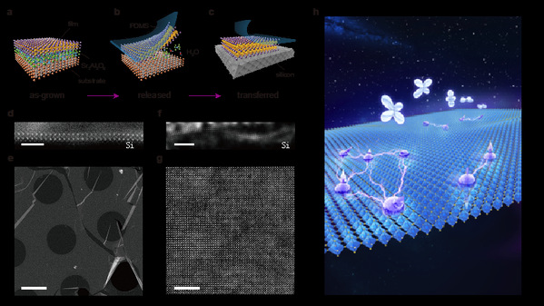
According to Xiaoqing Pan, unlike the pulsed laser deposition technology used by the Stanford research group, Prof. Yuefeng Nie 's research group used a thin film growth technique called molecular beam epitaxy to prepare two-dimensional oxide perovskite materials. By improving the in-situ monitoring technology and adopting a high-precision layer-by-layer growth method, Prof. Yuefeng Nie 's research group successfully achieved a breakthrough in the preparation and transfer of ultra-thin oxide perovskite films, and obtained high-quality oxide perovskite two-dimensional materials with atomic layer thickness. Prof. Peng Wang 's group used a variety of advanced spherical aberration correction transmission electron microscope structure analysis techniques to achieve electron microscope sample preparation, layer calibration and fine crystal structure characterization under the two-dimensional limit, and directly observed many novel phenomena of the perovskite BiFeO3 film under the two-dimensional limit. The realization of such a breakthrough benefits from the combination of advanced molecular beam epitaxial thin film growth technology and subatomic resolution electron microscopic analysis technology, and the close cooperation between researchers.
According to Yuefeng Nie, the movement of electrons in a material determines the performance of the material. In traditional two-dimensional materials such as graphene, the movement of electrons is relatively free and is not affected by other electrons; in many oxide perovskite materials, there is a strong interaction between electrons. The strong correlation between them has contributed to various novel quantum states including high-temperature superconductivity. To realize the two-dimensional material of perovskite, adding this strong correlation between electrons in the two-dimensional system is expected to obtain more abundant two-dimensional quantum phenomena and applications of strong correlation.
Peng Wang claimed that high-resolution electron microscopy technology played an important role in the discovery of perovskite oxide two-dimensional materials, which greatly benefited from the rapid development of spherical aberration correction technology and advanced characterization methods in the past decade. "We believe there will be more interesting and novel physical phenomena in this two-dimensional material on the microscopic scale waiting for us to explore and discover."
Graduate candidates Dianxiang Ji and Songhua Cai, contribute equally to the work. Yuefeng Nie, Peng Wang, and Xiaoqing Pan are co-corresponding authors. The academic leader of the cooperation team, Xiaoqing Pan, is Henry Samueli Chair Professor at the University of California at Irvine and Visiting Professor at Nanjing University. The research group of Professor E.Y. Tsymbal at the University of Nebraska-Lincoln and the research group of Professor Xiaoqing Pan at the University of California at Irvine participated in this project. This work is also supported by the Associate Professor Zhengbin Gu in sample preparation and Prof. Di Wu in the characterization of PFM samples. This work was supported by the National Key Basic Research and Development Program, the National Natural Science Foundation of China and the "Double Innovation Talents" project of Jiangsu Province, the College of Engineering and Applied Sciences at Nanjing University, the State Key Laboratory of Solid Microstructure Physics, Artificial Microstructure Science Strong support from the Collaborative Innovation Center for Technology and Jiangsu Key Laboratory of Functional Material Design Principles and Application Technology. Special thanks to the late academician Naiben Min for his enthusiastic encouragement and strong support for the establishment and development of the quantum material microstructure research center. The center was officially launched in 2016, aiming at the research on the microstructure and physical properties of quantum materials and the exploration and development for the generation of functional materials and devices.

(a-c) Schematic diagram of preparation and transfer of two-dimensional oxide perovskite thin films; (d-g) Characterization of subatomic resolution structures with different crystal orientations; (h) Prospect of rich and strongly correlated two-dimensional quantum states in two-dimensional oxide perovskite materials
(Source: NJU news web)

